05.11.1998
EP 427
FIRST
MIDTERM
1.
a-) Convert the
binary number (1101.0110)2 to hexadecimal; (2 Pts.)
b-) Convert the octal number (17)8 to
decimal; (2 Pts.)
c-) Convert the decimal number your student number
(last four numbers) to binary and octal; (3 Pts.)
d-) Convert the your last name (up to first five
letters) to decimal and binary. (3 Pts.)
2.
a-) Add the
following binary numbers; (5 Pts.)
1011010 1111 110.11
100101 11 101.01


 + + +
+ + +
b-) Perform the following binary subtractions (5 Pts.)
1101 10011 10.11
101 11001 11.01


 - - -
- - -
3.
a-) Find the
(r-1)’s complement of the given numbers (1011.011)2 and (0.4567)10.
(4 Pts.)
b-) Find the r’s complement of the given numbers
(101100.0110)2 and (12.68)10 (4 Pts.)
c-) Using the r’s complement subtract the given
numbers (1011)2 – (1100)2. (4 Pts.)
4.
Explain the basic
logic gates, complete two input logic gates truth table and their timing
diagrams.(10 Pts.)
5.
Simplify the
following functions;
a-) F=A(A+B)
(3 Pts.)
b-) F=AB+AB’+A’B
(3 Pts.)
c-) F=A+A’B (4
Pts.)
d-)F=(A+C’)(A+D)(B+C’)(B+D) (5 Pts.)
6.
Express the
following functions in a sum of minterms and a products of maxterms.
a-) F(A,B,C)=A(B’+C)+A’B (3 Pts.)
b-) F(A,B,C)=1
(3 Pts.)
c-) F(A,B,C,D)=ABC+A’BD’ (4 Pts.)
7.
Write the Boolean
equation of the given logic circuit and then draw its minimal NAND-NAND circuit
for F. (15 Pts.)
8.
A combinational
circuit has four inputs (A3A2A1A0)
and one output F. The output is equal to 1 when A2=A0.
a-) Obtain the truth table; (4 Pts.)
b-) Find the simplified output function in SOP form; (10 Pts.)
c-) Draw the simplified logic circuit. (4 Pts.)
9.
(Extra Question,
if you solve it, you will have one extra letter; i.e. CC Þ CB, in your final mark). Show that (AÅBÅC)’=AÅBÄC=AÄBÅC.
Dr.A.N.YAZICI
10.12.1998
EP 427
SECOND
MIDTERM
1.
a-) Simplify the
following equation using the Karnaugh mapping procedure and then implement it
with only three NAND gates. (5 Pts.)
F(a,b,c,d) = a’b’c’ +
bcd’ + ab’c’d’ + a’bc’d’ + bc’d’ + c’d’ + ab’c’
b-) Simplify the following function in (1) SOP and (2) POS
form and then implement them with either three NAND or NOR gates. (7 Pts.)
F
= ac’ + ace + ace’ + a’cd’ + a’d’e’
c-) Simplify the following function using don’t care
condition in (1) SOP and (2) POS form and then draw the logic circuits using
minimum number of basic logic gates. Indicate which of the logic circuit is
preferable. (7 Pts.)
F
= Σ ( 1, 4, 11, 14 )
d
= Σ ( 3, 6, 7, 9, 12, 13 )
d-) Implement the four Boolean functions listed using
three half-adder circuits. (6 Pts.)
D
= A Å B Å C
E
= A’BC + AB’C
F
= ABC’ + (A’ + B’ ) C
G
= ABC
e-) Design of a logical device that receives a
four-bit binary number A4A3A2A1,
and is to indicate the prime numbers. (5 Pts.)
2.
Suppose that a
computer and printer system uses 4-bit odd parity generator and checker;
a-) Tabulate the truth table of parity generator. (4
Pts.)
b-) Write and simplify the output function of parity
generator using any simplification technique which you learned. (6 Pts.)
c-) Implement the logic circuits of parity generator
and checker in the simplest form. (6 Pts.)
d-) Discuss in which conditions parity checker gives
error. (4 Pts.)
3.
Design of a combinational logical device that is convert a
decimal digit from 6,3,2,-1 BCD code to 8,4,2,1 BCD code. (20 Pts.)
4.
Design a 8421 BCD
subtractor using full-adder(s) and (if necessary) basic logic gates. (30 Pts.)
Dr.A.N.YAZICI
07.01.1999
EP 427
FINAL
EXAMINATION
1 a-) Convert the binary number
(111101000.0111)2 into an octal, a decimal and a hexadecimal
number. b-) Convert (25223)6
to a decimal number.
c-) Given a decimal integer number of n digits, how
many digits are required to represent the same number in base 2 and 16 ?
d-) Using the (r-1)’s complement subtract the given
numbers (1011)2 – (1100)2.
2 a-) Find the Boolean sum of the two
functions by adding the values of the corresponding cells of their maps.

b- Find the Boolean
product of the two functions by adding the values of the corresponding cells of
their maps.

3.
Design a
system-called a parallel binary comparator that compares the 4-bit string A (A3A2A1A0)
to the 4-bit binary string B (B3B2B1B0).
If the string are exactly equal, provide a high-level output to drive a warning
buzzer.
4.
Implement the
function F(a,b,c,d)=åm(1,2,4,5,6,9,10,11,13) using one 8-bit multiplexer.
How many IC packages (7400) would be required to implement the function with
NAND gates ?
5.
Redefine the carry
propagate and carry generate as follows

Show that the output carry and output
sum of a full-adder becomes
6.
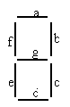 Design of a
BCD-to-seven-segment decoder circuit using a BCD-to-decimal decoder (4 x 10
decoder) and, if necessary, basic logic gates. A BCD-to-seven-segment decoder
is a combinational circuit that accepts a decimal digit in BCD and generates
the appropriate outputs for selection of segments in a display indicator used
for displaying the decimal digit. The seven outputs of the decoder (a, b, c, d,
e, f, g) select the corresponding segments in display as shown in below figure.
Design of a
BCD-to-seven-segment decoder circuit using a BCD-to-decimal decoder (4 x 10
decoder) and, if necessary, basic logic gates. A BCD-to-seven-segment decoder
is a combinational circuit that accepts a decimal digit in BCD and generates
the appropriate outputs for selection of segments in a display indicator used
for displaying the decimal digit. The seven outputs of the decoder (a, b, c, d,
e, f, g) select the corresponding segments in display as shown in below figure.
Dr.A.N.YAZICI
21.04.1999
EP 427 DIGITAL
ELECTRONICS
FIRST MIDTERM
Time Duration : 120 Mins.
1.
a-) Convert the
hexadecimal number (23AB.08CD)16 to octal; (2 Pts.)
b-) Convert the BCD number (000100100011.00000110)BCD
to decimal; (2 Pts.)
c-) Convert the decimal number (153.513)10
to a three digit octal fraction number. (2 Pts.)
2.
Perform the
following additions, subtractions and multiplications. (14 Pts.)


 1111.110 BABA 725.01 110.11 1453 1101 61

 101.011 DEDE 601.17
 11.01 1271 101 63
(
)2 ( )16 ( )8 ( )2 ( )8 ( )2 (
)7
3.
a-) Find the
(r-1)’s complement of the given numbers (0101.0110)2 and (10.257)10.
(4 Pts.)
b-) Find the r’s complement of the given numbers
(101100.0110)2 and (12.68)10 (4 Pts.)
c-) Using the r’s complement subtract the given
numbers (1011)2 – (1100)2. (4 Pts.)
4.
Simplify the
following functions using Boolean simplification techniques,
a-) f=a(a+b)+
a’(a+b)’ (5 Pts.)
b-) f=a+abc+ab+a’bc (5 Pts.)
c-) f=(a+c’)(a+d)(b+c’)(b+d)
(6 Pts.)
5.
For the given
circuits;
a-) Write the Boolean output equation, (6 Pts.)
b-) Obtain the minterms and maxterms of the function,
(6 Pts.)
c-) Using K-map simplify it and (6 Pts.)
d-) Draw the simplified logic circuit. (4 Pts.)
6.
Simplify the
following function using don’t care condition in (1) SOP and (2) POS form and
then draw the logic
circuits using minimum number of basic logic gates. Indicate which of
the logic circuit is
preferable. (10 Pts.)
F
= Σ ( 1, 4, 11, 14 )
d
= Σ ( 3, 6, 7, 9, 12, 13 )
7.
In order to obtain
four bit parity generator,
a-) Complete the truth
table of it; (4 Pts.)
b-) Find the simplified output function in SOP form; (6 Pts.)
c-) Draw the
simplified 4-bit Even Generator Logic circuit. (4 Pts.)
d-) Discuss can
you obtain 8-bit Even Generator using 4-bit Even Generator. How? (6 Pts.)
Good
Luck Dr.A.N.YAZICI
20.06.1999
EP
427 Digital Electronics
Final Exam (Time Duration : 100 mins.)
(Choose only one of them
after question 5)
1.
Design a decimal
arithmetic unit with two selection variables, V1 and V0,
and two BCD digits, A and B. The unit should have four arithmetic operations
which depend on the values of the selection variables as shown below table.
|
V1
|
V2
|
Output function
|
|
Use block diagram for all used MSI circuit
|
|
0
|
0
|
A + 9’s complement of B
|
|
0
|
1
|
A + B
|
|
1
|
0
|
A + 10’s complement of B
|
|
1
|
1
|
A + 1 (add 1 to A)
|
2. A combinational circuit is specified by the following three Boolean
functions; F1 = x’y’ + xz’,
F2 = y’ + x’z, F3
= x’y + yz. Implement the
circuit with a decoder which constructed with NAND gates and minimum number of external NAND gates.
3. Implement the following Boolean function F(A,B,C,D)=Σ(1,3,4,11,12,13,14,15) with a 4 x 1 multiplexer
and minimum number of necessary external gates. Connect inputs A and B to the selection lines of used multiplexer. The input
requirements for the four data lines (I0, I1, I2
and I3) of multiplexer will be function of variables C and D. These values are obtained by expressing F as a function of C and D for each of the four cases when AB = 00, 01, 10, 11. These function may have to be implemented with external gates.
4. An 8 x 1 multiplexer has A, C and D connected to the selection inputs s2, s1
and s0, respectively. The data inputs , I0 through I7
are as follows: I0=I3=I5=I6=B
and I1=I2=I4=I7=B’.
Find the function and then simplified it. Draw the simplified function using
minimum number of basic logic gates.
Please choose only one of them after question 5.
5. List the PLA program table for the BCD-to-excess-3 code converter.
6. Design a 4-line to 2-line priority encoder. Include an output E to
indicate that at least one input is a 1.
7. Construct a 5 x 32 decoder with four 3 x 8 decoder / demultiplexers with
an enable input and a 2 x 4 decoder. Use block diagrams of all necessary
circuits.
8. Draw the logic diagram of a 2 x 4 decoder using only minimum number of
NOR gates.
9. The following circuit of below figure has following values for variable
input V and data inputs A and B. In each case, determine the values of the
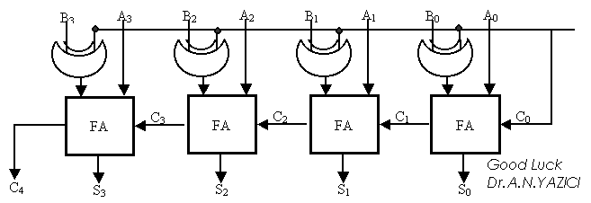
outputs S3, S2, S1, So, and C4.
|
V
|
A
|
B
|
|
0
|
0111
|
0110
|
|
0
|
1000
|
1001
|
|
1
|
1100
|
1000
|
|
1
|
0101
|
1010
|
17.11.1999
EP 427 Digital Electronics
First Midterm
(Time Duration : 110 Mins.)
- a-) Perform the following binary arithmetic operations (8 p)
i-) 1101 + 1011 (1p) ii-)
1100 – 1001 (1p) iii-) 1001 x 110
(3p) iv-) 1001 ¸11 (3p)
b-) Perform each of the following operations with 2’s
complement system
i-) 11011001 + 11100111 (2p) ii-)
01100101 – 11101000 (2p)
c-) Perform the following arithmetic operations
i-) (AA)16 + (FF)16 (2p) ii-) (FD)16 – (8E)16
(2p) iii-)
(25)8 x (17)8 (4p)
2.
Sensors are used to monitor the pressure and the temperature
of a chemical solution stored in a vat. The circuitry for each sensor produces
a HIGH voltage when a specific maximum value is exceeded. An alarm requiring a
LOW voltage input must be activated when either the pressure or the temperature
is excessive.
i-) Tabulate the truth table of the system. (6p)
ii) Design a circuit for this application. (6p)
- Simplify each of the following expressions to a minimum form
i-) F1=
A’B(C’D’ + C’D) + AB(C’D’ + C’D) + AB’C’D (5p)
ii-) F2=
(A + B’)(A + C’)(A’ + B’ + C) (5p)
iii-) F3= A+A’B (5p)
- For the given functions, perform the following Boolean arithmetic
operations and then simplify them suing K-map and finally implement
simplified function using minimum number of gates.
i-)  (10p)
(10p)
ii-)  (12p)
(12p)
- Implement a full-subtractor with two-half adders, one OR gate and
one INVERTER. (15p)
- When the input waveforms (A,B,C,D) are supplied to a logic circuit,
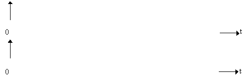
the output waveform (F) is obtained as shown in figure 1. Implement the
logic circuit inside the box using minimum number of gates. (16p)
Dr.A.N.YAZICI
30.12.1999
EP 427 Digital Electronics
Second Midterm (Time Duration : 120 Mins.)
1.
a-) Design a combinational logic circuit that converts a
decimal equivalent from 6461 code to 8421 code using minimum number of
necessary logic gates.
b-) Implement
the same circuit using a decoder which is constructed with NAND gates and
minimum number of necessary basic logic gates.
2.
Using multiplexers, design a circuit that compares 2-bit two
binary numbers A (A1A0) and B (B1B0).
3.
Design a binary multiplier that multiples a 4-bit number B=B3B2B1B0
by a 3-bit number A=A2A1A0 to form the product
C=C6C5C4C3C2C1C0.
Hint : This logic circuit
can be constructed with AND gates and two 4-bit parallel adders. The AND gates
are used to form the products of pairs of bits (i.e. A0 times B0
® A0B0). The parallel adders are used to
sum the partial products formed by the AND gates.
- List the PLA program table for the BCD-to-2’s complement of a BCD
digit.
- The waveforms in given figure are applied to the J-K, and clock
pulse input for AND+NOR constructed J_K flip-flop. Firstly tabulate the Q
and Q’ values as a function of possible input combinations and then draw
the output waveforms of Q and Q’ for the given inputs. (Assume that all of
the timing parameters are zero and initial value of Q=0).
- Sketch the output waveforms Q
and Q’ of an R-S latch which is constructed with NOR gates for the
given input waveforms. (Assume that tr=0, tf=0, tp??=10
ns, each time division in given figure is 10 ns and Q is initially
1).
Good Luck
Dr.A.N.YAZICI
….01.2000
EP 427 Digital Electronics
Second Make-Up Exam.
Time Duration :100 Mins.
- Design a decimal arithmetic unit with two selection variables, V1
and V0, and two BCD digits, A and B. The unit should have four
arithmetic operations which depend on the values of the selection
variables as shown below table.
|
V1
|
V2
|
Output function
|
|
Use block diagram for all used MSI circuit
|
|
0
|
0
|
A + 9’s complement of B
|
|
0
|
1
|
A + B
|
|
1
|
0
|
A + 10’s complement of B
|
|
1
|
1
|
A + 1 (add 1 to A)
|
2. A combinational circuit is specified by the following three Boolean
functions; F1 = x’y’ + xz’,
F2 = y’ + x’z, F3
= x’y + yz. Implement the
circuit with a decoder which constructed with NAND gates and minimum number of external NAND gates.
3. Implement the following Boolean function F(A,B,C,D)=Σ(1,3,4,11,12,13,14,15) with a 4 x 1 multiplexer
and minimum number of necessary external gates. Connect inputs A and B to the selection lines of used multiplexer. The input
requirements for the four data lines (I0, I1, I2
and I3) of multiplexer will be function of variables C and D. These values are obtained by expressing F as a function of C and D for each of the four cases when AB = 00, 01, 10, 11. These function may have to be implemented with external gates.
4.
Design a binary multiplier that multiples a 4-bit number B=B3B2B1B0
by a 3-bit number A=A2A1A0 to form the product
C=C6C5C4C3C2C1C0.
Hint : This logic circuit
can be constructed with AND gates and two 4-bit parallel adders. The AND gates
are used to form the products of pairs of bits (i.e. A0 times B0
® A0B0). The parallel adders are used to
sum the partial products formed by the AND gates.
Good Luck
Dr.A.N.YAZICI
19.01.2000
EP 427 Digital Electronics
Final Exam
Time Duration :120 Mins.
- An 8x1 multiplexer has A, B, and C connected to the selection inputs S2, S1, and
S0, respectively. The data inputs, I0 through I7 are as follows : I0=I2=I3=I5=I6=D,
I1=1 and I4=I7=0.
a-) Complete the truth
table.
b-) Simplify the function in
SOP and POS forms using K-map.
c-) Draw the simplest
function using minimum number of necessary basic logic gates.
d-) Explain the goal of this
circuit.
- Design a logic circuit (Quadruple 4-to-1
line multiplexer) that selects only one of the inputs A, B, C or D at the
output Y using minimum number of necessary input selection lines and
enable input. All of the input numbers have four bits (i.e. A3A2A1A0)
so output number has also four bits Y3Y2Y1Y0.
- Design a combinational logic circuit
either in block diagram or not that converts a decimal digit from its
decimal number system to binary number system when you press the key of
decimal digit.
- Design a logic circuit that detects the
errors occur when a binary information transferring from a computer to a
printer. Restrict that the long of binary information are four bits.
- The following inputs are applied to the
negative edge-triggered R-S flip flop.
a-) Explain the operational
principle of edge-triggered R-S flip flop.
b-) Draw the output
waveforms of both output (Assume that initial position of Q=HİGH and all of the
timing parameters are equal to zero).
Good Luck
Dr.A.N.YAZICI
15.11.2000
EP 427 Digital Electronics
First Midterm
Time Duration :120 Mins.
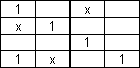
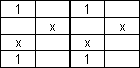
1- ) Simplify the following function using don’t care conditions in both SOP
and POS form.
¦(a,b,c,d)=å(0,2,4,5,7,13)
d(a,b,c,d)=å(6,8,9,10,14)
2-)
Implement the logic circuit of the following functions using minimum number of
logic gates
(Only one input is available in complement form).
i-) F1(A,B,C,D) = A(B’C’ + BCD) +
B’D’ + A’(BC’D + B’C) + AB’C’D
ii-) F2(A,B,C,D)
= (B’+D’)(A’+C’+D)(A+B’+C’+D)(A’+B+C’+D’)
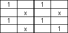
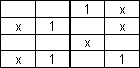
3-) Find
the simple form of the following Boolean function operations.
¦1(w,x,y,z)=å(0,2,4,6,9,11) ¦2(w,x,y,z)=Õ(0,1,4,13,15)
d1(w,x,y,z)=å(1,13,15) d2(w,x,y,z)=å(2,7,9,10)
|
|
1
|
|
1
|
x
|
1
|
1
|
x
|
1
|
|
1
|
1
|
1
|
x
|
1
|
|
1
|
|
4 -) Design a logic circuit that finds odd and even decimal numbers between 0
and 15.
5-)
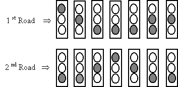
Design a logic circuit that controls traffic lights in two-roads using
following cycles.
Good Luck
Dr.A.N.YAZICI
29.11.2000
EP 427 Digital Electronics
Second Midterm
Time Duration :90 Mins.
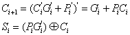
1-) Show that carry four (C4) in a full-adder
circuit (for 4-bits two-numbers A3A2A1A0
and B3B2B1B0) can
also be given in the form
of
C4=G3 + F3G2 +
F3F2G1 + F3F2F1G0
+ F3F2F1F0C0
2-) Design a
combinational logic circuit that is convert a decimal digit from 8421 code to
2214 code using a decoder and if necessary the other basic logic gates.
3-) Design a logic circuit of a keyboard that
converts decimal digits (0,1,2,…,9) to its binary number
system when you press the
keys on the keyboard.
4-) a-) Implement the following Boolean function F(A,B,C,D) = P (1,3,4,7,8,9,11,12,13,15) with a 4x1
multiplexer and minimum number of necessary basic
logic gates.
b-) Implement the same function with also 8x1 multiplexer
and the other necessary basic logic gates. Indicate which of them becomes economic then the other in your
chosen system.
Good Luck
Dr.A.N.YAZICI
..…./…../2000
EP 427 Digital Electronics
Final Exam
Time Duration :90 Mins.
1-) Determine the minimal POS and SOP realization
for the following functions.
i-) f(a,b,c,d)
= å(0,2,8,9) + åd(1,3)
ii-)
f(a,b,c,d) = å(1,7,11,13) + åd(0,5,10,15)
2-) Consider the following functions
f1(x,y,z)=å(0,1,2,4,5,7)
f2(x,y,z)=P(0,2,3,4,5,7)
a-) Find the minimal
AND-OR realization of f1 and a minimal OR-AND realization of f2.
b-) Implement the both
functions using a decoder and if necessary the other basic logic gates.
3-) Implement the following function with
an 8x1 multiplexer
F(A,B,C,D,E)= A’B’C’DE’ + AB’C’ + ABC’DE + A’BCD’E’ + AB’C
+ A’B’C’D’E +
ABC’D’E’ +
ABC’DE’ + A’BCDE + ABC’D’E
4-) a-) List the PLA program table for the 8421-to-2214 code converter.
b-) Indicate how many basic logic gates are required to
obtain the logic circuit of this PLA device.
Good Luck
Dr.A.N.YAZICI